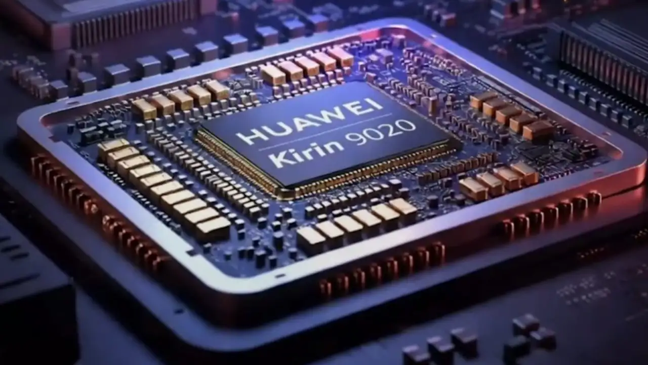
Huawei has unveiled its latest smartphone processor, the Kirin 2026, marking a significant advancement in semiconductor design. Set to power the company’s upcoming flagship Mate series handsets launching in autumn 2026, the chip delivers major performance and efficiency gains while operating on the same manufacturing process node as its predecessor, the Kirin 9030 Pro.
This achievement is particularly noteworthy amid ongoing U.S. sanctions that restrict Huawei’s access to cutting-edge extreme ultraviolet (EUV) lithography equipment, highlighting China’s push toward semiconductor self-reliance through innovative architectural approaches rather than pure process scaling.
The core innovation behind the Kirin 2026 is Huawei’s LogicFolding architecture, introduced alongside the company’s Tau (τ) Scaling Law. Rather than shrinking transistors further, which requires increasingly expensive and restricted fabrication technologies—LogicFolding optimizes circuit layout by “folding” logic elements in ways that shorten interconnects and reduce overhead.
Key technical improvements include:
55% increase in transistor density approximately 53.5% in some reports compared to the Kirin 9030 Pro, reaching around 238 million transistors per square millimeter on the same SMIC 7nm-class node. This density rivals what TSMC’s 3nm or Intel’s 18A processes achieve through traditional scaling.
Wire length shortened by 30%, reducing resistive and capacitive loads on signals.
Clock-buffer count reduced by over 50% and clock skew cut by 25%, enabling more efficient high-frequency operation.
Power consumption reduced by 41% at the same performance level, with a 5.6% reduction in power density. Tests at 25°C and 0.9V highlight these efficiency gains.
These changes allow the chip’s CPU cores expected to use an updated Taishan V4 architecture to reach higher clocks, potentially up to 3.1 GHz, compared to the previous generation, while maintaining or improving overall efficiency.
The LogicFolding design is part of Huawei’s broader Tau (τ) Scaling Law, presented by He Tingbo, Huawei’s “chip queen” and president of its semiconductor business. This law emphasizes multi-level co-optimization across devices, circuits, chips, and systems to compress signal propagation delays and sustain performance improvements.
Huawei claims it has already designed and mass-produced 381 chips based on this approach. Looking ahead, the company projects that high-end chips using these techniques could achieve transistor densities equivalent to a 1.4nm process by 2031, with further frequency scaling toward 4 GHz and beyond.
The Kirin 2026 represents more than just a smartphone SoC upgrade. It demonstrates a viable path for China to advance in semiconductors despite export controls on advanced tools. By focusing on design innovations like 3D-like stacking elements via wafer-to-wafer hybrid bonding in some descriptions and smarter layouts, Huawei aims to close the gap with global leaders.
Critics note that the density claims involve specific accounting methods and that the chip remains a catch-up effort rather than a outright leap, but real-world testing in the Mate 90 series will ultimately validate the gains in battery life, sustained performance, and AI capabilities.
The Kirin 2026 is expected to feature improvements across CPU, GPU, and NPU subsystems, supporting enhanced on-device AI, better gaming, and improved photography processing. Huawei’s ecosystem, including HarmonyOS, will likely be optimized to take full advantage of the new silicon.
As global chip competition intensifies, Huawei’s progress underscores the growing importance of architectural ingenuity alongside manufacturing prowess. The Kirin 2026 could strengthen the company’s position in the premium smartphone market and serve as a proof point for China’s broader tech ambitions.
Stay tuned for hands-on benchmarks when the Mate 90 series arrives later in 2026. This chip may not rewrite Moore’s Law entirely, but it shows that clever design can still deliver substantial leaps even under constraints.